About the Fraunhofer Institute for Photonic Microsystems
The Fraunhofer Institute for Photonic Microsystems IPMS in Dresden, Germany, is one of the leading international research and development service providers in the field of optical sensors and actuators, integrated circuits, microsystems (MEMS/MOEMS) and nanoelectronics. The IPMS develops and researches components, systems and technologies that find application in smart industrial solutions, mobility as well as bio and health technologies. This is made possible from conception to pilot production for market entry and is ISO9001 certified. Moreover, it conducts research on memory technologies, quantum and neuromorphic computing and sustainable microelectronics. Fraunhofer IPMS has at its disposal three state-of-the-art 200 and 300 mm clean rooms and a total of four development sites in Dresden, Cottbus and Erfurt.
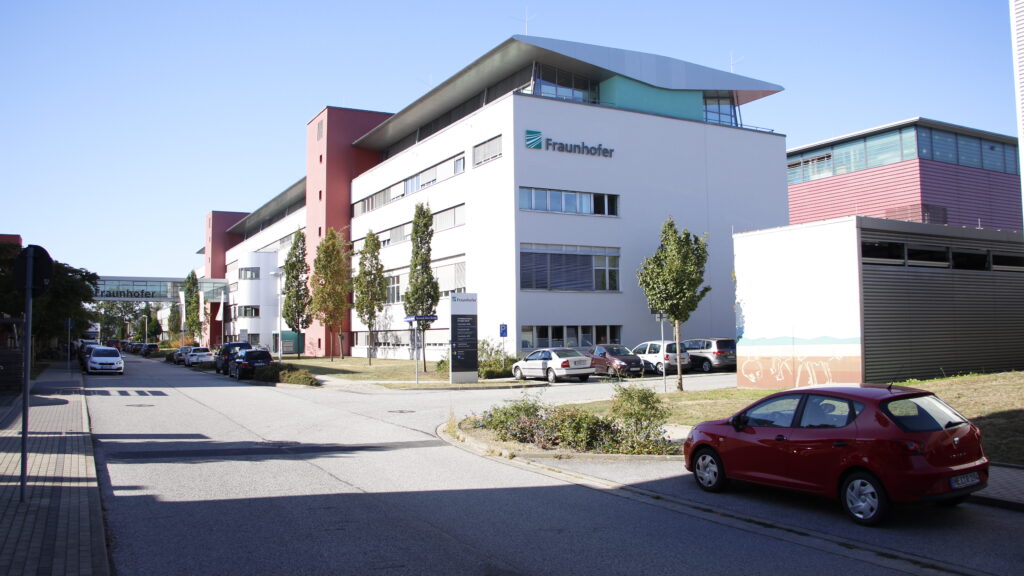
Office building of Fraunhofer IPMS
Fraunhofer IPMS is Part of FMD. For the first time, 13 institutes from the two research organizations, Fraunhofer and Leibniz, are combining their expertise under one virtual umbrella, thus creating a new quality to the research and development of micro- and nanosystems. With more than 2,000 scientists, the FMD is one the world’s largest R&D network of its kind. With its unique diversity of expertise and infrastructure at the institutes, it is helping Germany and Europe to further expand their leading position in research and development.
The Fraunhofer-Gesellschaft in Germany
Fraunhofer IPMS is a part of the Fraunhofer-Gesellschaft, based in Germany, the world’s leading applied research organization. Prioritizing key future-relevant technologies and commercializing its findings in business and industry, it plays a major role in the innovation process. Founded in 1949, the recognized non-profit organization currently operates 76 institutes and research units throughout Germany. Currently around 32,000 employees, predominantly scientists and engineers, work with an annual research budget of about 3.4 billion euros, 3.0 billion euros of which is designated as contract research.
Development of customer-specific sensors and actuators at Fraunhofer IPMS
For the ThrombUS+ Project mainly the business unit “Acoustic Sensors and Systems” at Fraunhofer IPMS is involved and works on ultrasound sensors and actuators and their integration into miniaturized devices and systems. By using microsystems (MEMS, CMOS), the functionality of many products can be enhanced. Especially for applications in medical technology, commercial sensor solutions often do not meet the requirements. Fraunhofer IPMS develops custom-specific solutions tailored to the customer’s application.
Fraunhofer IPMS is a high-quality development partner when it comes to making sensors smaller, more intelligent, more individualized or more functional. Our ultrasound sensors offer state-of-the-art properties such as:
- Miniaturization (smaller dimensions, lower consumption, CMOS compatible, hetero integration…)
- Advanced functionality (connectivity, multi-sensor solutions, …)
- Novel materials (robust, no fatigue, RoHs compatible, …)
- Scalable manufacturing

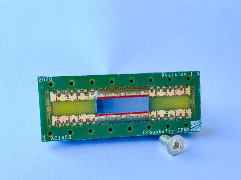
Section of a wafer with 1D linear CMUT array
Ultrasonic Sensors from Fraunhofer IPMS
The measurement method of ultrasonic sensors is based on the transmission of ultrasonic waves and the detection of echo signals from the environment. Capacitive micromachined ultrasonic transducers (CMUT) are miniaturized sensor structures whose electrostatic operating principle enables both the transmission and detection of ultrasonic waves. This new generation of ultrasonic transducers is manufactured using semiconductor technology processes and thus enables great flexibility in sensor design with high precision and reproducibility in the manufacturing process for single and multi-channel systems.
Features of the CMUTs at Fraunhofer IPMS:
- wide range of elements with different frequencies (> 400 kHz)
- high acoustic bandwidth (> 100% in immersion; > 20% in air)
- high spatial resolution (submillimetre scale)
- low acoustic losses
- extreme miniaturisation (≤ 1 mm³)
Contribution to the ThrombUS+ project
In the project, Fraunhofer IPMS is developing ultrasound transducer arrays for the portable component, which will enable continuous monitoring of DVT (Deep Vein Thrombosis) directly on site. We are focusing on our CMUTs (Capacitive Micromachined Ultrasonic Transducers), which are MEMS-based transducers considered the next generation of medical ultrasound devices. Their advantages open up the possibility of developing a completely new diagnostic system.
In combination with on-chip sensor control and embedded AI, intelligent MUT systems will be available in the future for integration into sensor networks for multimodal environmental monitoring.
These miniaturized systems benefit from reliable manufacturing processes, which enable cost-effective and high-volume production. In addition, the manufacturing process and the CMUT elements do not contain any toxic substances (including lead), the Fraunhofer IPMS capacitive transducers are therefore RoHS (“Reduction of Hazardous Substances”) compliant. MUTs are manufacturable for a wide range of ultrasound frequencies, enabling application-specific ranges and resolving power. Sensor solutions can be manufactured in single-channel structures as well as in arbitrary two-dimensional array structures. The latter enable the application of imaging techniques for environmental monitoring.
Investment in our future: Green ICT – Sustainable Microelectronics
High-tech developments and global connections to customers also come with great responsibility. Fraunhofer IPMS is aware of this. Sustainability is important to us
Currently, the institute wants to take steps towards a green microelectronics future both at its own site and during the industry-wide processes of electronics production. This is mainly done by participating in a project called (Green ICT). All results are also transferred to customers. Research is being carried out on:
- Optimization of material consumption in the area of wet processes and lithography by reducing resource requirements or evaluation of processes using alternative material types
- Optimization of waste gases from special process steps, minimization of waste gas pollution in the environment


